5 things to know about PCB footprints
4.8 (515) · € 28.50 · En Stock
.jpg)
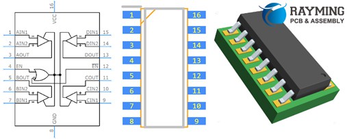
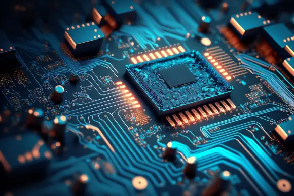
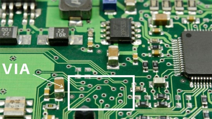
Each component placed on the sides of a printed circuit board must have its own footprint.
The Difference between Footprints and Land Patterns in PCB - RAYPCB
Designing PCBs: SMD Footprints - SparkFun Learn
An Introduction to Printed Circuit Boards

Ultimate Guide to PCB Layout Design Considerations
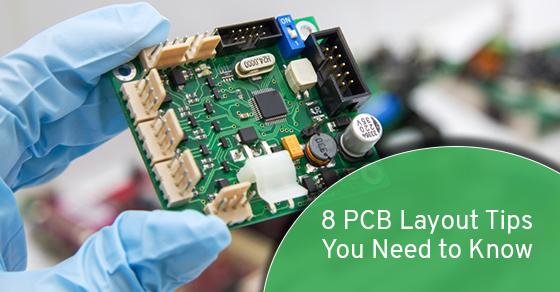
8 PCB Layout Tips You Need to Know
Three Ways to Hack a Printed Circuit Board - IEEE Spectrum

What are different layers in PCB Footprint.#orcad #allegro

Four Pillars of PCB Design for Successful IoT Products
How to Design a PCB Layout

Understanding PCB Footprints - The Ideal PCB Land Pattern (QFN

Understanding the importance of PCB footprints in electronic
Tu pourrais aussi aimer


Proposer des recherches


© 2018-2024, thefforest.co.uk, Inc. ou ses affiliés