
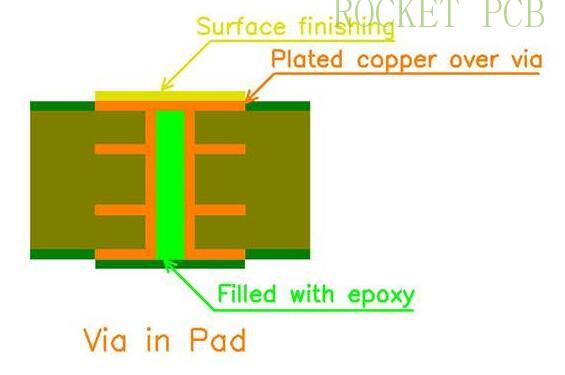
PCB Via Filling/Plugging is a process where the Via hole is filled with solder mask or resin to improve the reliability of the printed circuit board.

PCB production – Eurocircuits
PCB Via Filling Explained
pcb - Vias directly on SMD pads? - Electrical Engineering Stack

Via (electronics) - Wikipedia
Technical Analysis Of Vippo Pcb/ Pofv Pcb
To Fill or Not to Fill Vias? - Rush PCB
My PCB fab (JLCPCB) filled or covered all my vias and through

PCB Vias - Everything You Need To Know
My PCB fab (JLCPCB) filled or covered all my vias and through

Understanding via in pad in PCB-types, advantages, process
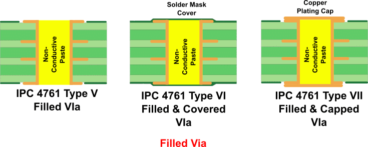
To Fill or Not to Fill Vias? - Rush PCB
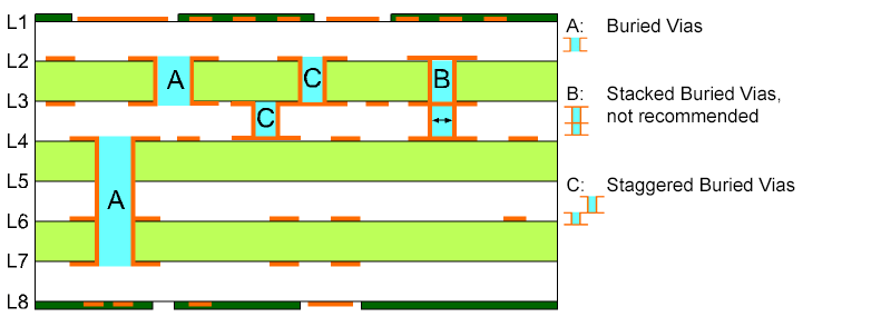
Blind Vias & Buried Vias - Multi Circuit Boards
Tu pourrais aussi aimer


© 2018-2024, thefforest.co.uk, Inc. ou ses affiliés