Trace PCB: A Comprehensive Guide
4.5 (793) · € 34.00 · En Stock
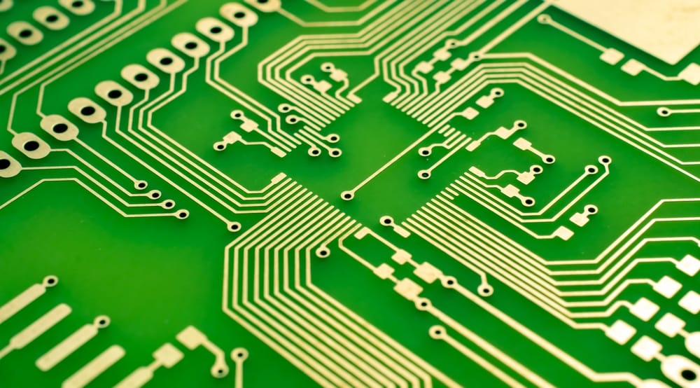
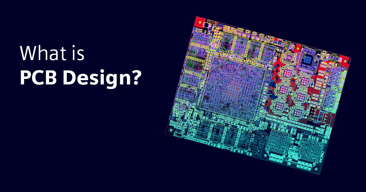
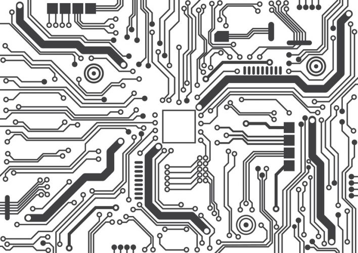
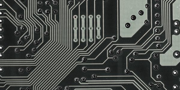
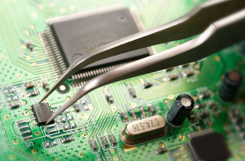
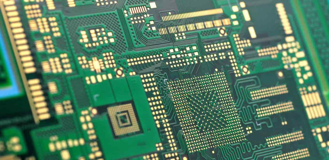
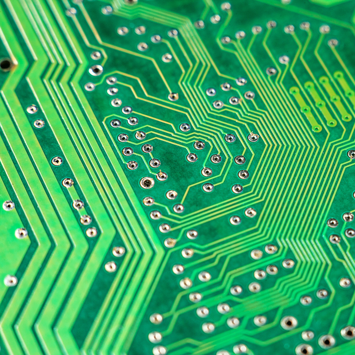
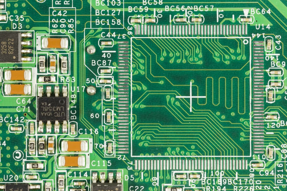
A PCB trace is a highly conductive track that is used to connect components on a printed circuit board. The traces are commonly made of copper and are fabricated during the etching process of a PCB. This article delves into the explanation of PCB trace, its vital components, and its significance to PCB design and fabrication.
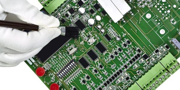
Cleaning Circuit Boards: A Comprehensive Guide
PCB Design Steps & Complete Guide
Ultimate Guide to PCB Layout Design Considerations

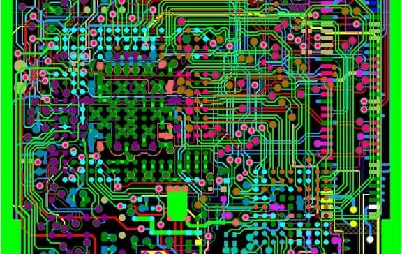
Everything you want to know about PCB trace - IBE Electronics

The Ultimate Guide to PCB Design and Fabrication in Delhi: Shree Ram Electronics Leading the Way, by Shree Ram Electronics
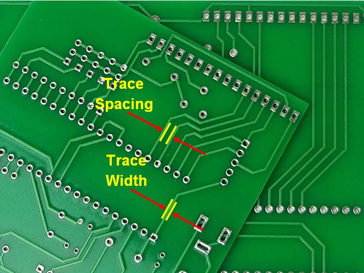
Best Guide To PCB Traces: Width, Thickness And Design Fix Recommendations - Jhdpcb
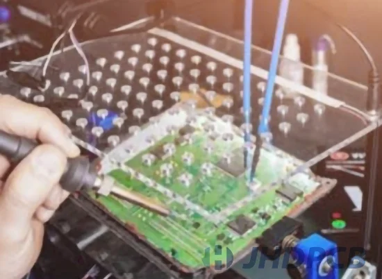
Ultimate Guide to Benchtop PCB Rework & Repair
PCB Plating Techniques: The Ultimate Guide for Success
PCB Current Trace Width: A Complete Guide

Why can't PCB traces be too long? - IBE Electronics

PCB Pitch: The Ultimate Guide to Crafting an Effective PCB Pitch - MorePCB
Mastering the Art of PCB Design: A Comprehensive Guide, by Faouzi NAJI
How to Design a PCB Layout: A Comprehensive Guide